
Page 28 - 2025S
P. 28
UEC Int’l Mini-Conference No.54 21
Inductorless 5.405 GHz Fractional-N PLL for RF
Synthesis with 5.6 mW Power Consumption
∗
Thi Viet Ha NGUYEN , Trong-Thuc HOANG, and Cong-Kha PHAM
Department of Network and Computer Engineering
The University of Electro-Communications, Tokyo, Japan
Keywords: Phase Locked-Loop, fractional-N PLL, ∆Σ noise, multi-loop PLL, introducless, RF synthesis.
1 Introduction
For energy efficient RF sythesis in IoT and mo-
bile applications, this work introduces an enhanced
Fractional-N Phase Locked Loop (PLL) architecture
in Figure 1. The design achieves a power consump- Figure 2: The schematic of VCO.
tion of less than 5.6 mW while delivering superior
performance in terms of phase noise and loop band-
width. To mitigate ∆Σ quantization noise, a novel
adaptive digital noise filter is implemented replacing
the conventional synchronous delay line. A multi-
loop PLL structure is incorporated to improve fre-
quency accuracy and minimize jitter. Furthermore,
a high resolution digital phase detector (DPD) is uti- Figure 3: ∆Σ modulation architecture in Fraction-N
lized to reduce phase variation. Implemented in a PLL.
180 nm CMOS process, the PLL exhibits an in-band
phase noise of less than −105 dBc/Hz, an integrated
jitter of approximately 1 ps rms , and a loop band-
width exceeding 15 MHz. These results demonstrate
the proposed PLL’s suitability for high-precision,
low-power wireless communication systems [1].
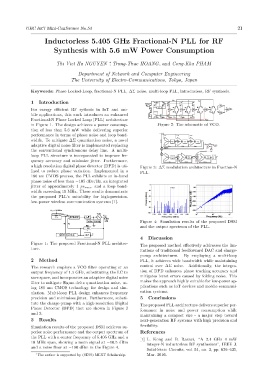
Figure 4: Simulation results of the proposed DSM
and the output spectrum of the PLL.
4 Discussion
Figure 1: The proposed Fractional-N PLL architec- The proposed method effectively addresses the lim-
ture.
itations of traditional feedforward DAC and charge-
pump architectures. By employing a multi-loop
2 Method PLL, it achieves wide bandwidth while maintaining
The research employs a VCO filter operating at an control over ∆Σ noise. Additionally, the integra-
output frequency of 1.5 GHz, substituting the LC to tion of DPD enhances phase tracking accuracy and
mitigates burst errors caused by folding noise. This
save space, and incorporates an adaptive digital noise
filter to mitigate Sigma delta quantization noise, us- makes the approach highly suitable for low-power ap-
ing 180 nm CMOS technology for design and sim- plications such as IoT devices and mobile communi-
ulation. Multi-loop PLL design enhances frequency cation systems.
precision and minimises jitter. Furthermore, substi- 5 Conclusions
tute the charge-pump with a high-resolution Digital The proposed PLL architecture delivers superior per-
Phase Detector (DPD) that are shown in Figure 2 formance in noise and power consumption while
and 3.
maintaining a compact size - a major step toward
3 Results next-generation RF systems with high precision and
Simulation results of the proposed DSM achieves su- flexibility.
perior noise performance and the output spectrum of References
the PLL with a center frequency of 5.405 GHz and a [1] L. Kong and B. Razavi, “A 2.4 GHz 4 mW
10 MHz span, showing a main signal at −10.5 dBm integer-N inductorless RF synthesizer”, IEEE J.
and a noise floor at −100 dBm in the Figure 4.
Solid-State Circuits, vol. 51, no. 3, pp. 626–635,
∗ The author is supported by (SESS) MEXT Scholarship. Mar. 2016.