Page 79 - 2024S
P. 79
72                                                                UEC Int’l Mini-Conference No.52


               UEC International Mini-Conference No.52
                                       Electron Beam Fabrication of Phase Hologram
                                           Tonmoy Hasan CHOWDHURY  , Yoko MIYAMOTO
                                                                 *
                                  * Department of Engineering Science, the University of Electro-Communications
                                    * Institute for Advanced Science, the University of Electro-Communications
                                            1-5-1 Chofugaoka, Chofu, Tokyo, 182-8585, Japan
                  Keywords: Electron beam fabrication, optical vortex array, phase hologram, classical and quantum information communication.
               Objectives:
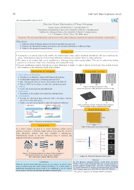
                   1. Fabricate phase hologram using an electron beam fabrication process.
                   2. Evaluate the fabricated hologram and observe the intensity distribution of diffracted light.
                   3. Relate to the proposed research theme.
                                                       Background
               ü A hologram is an optical element that modifies the incident light's phase and/or amplitude distributions. We aim to fabricate the
                 phase-only holograms using the electron beam fabrication technique on a polymer layer on a glass substrate.
               üThe phase of the incident light can be modified by a reflecting surface with varying heights. This can be achieved by writing
                 patterns on an electron-beam resist, developing, and coating with metal.
               üAccurate modification of phase depends on accurate fabrication of height. To achieve this we need precise data on how electron
                 dose translates to the fabrication depth of the polymer.
                             Fabrication of Hologram                         Holographic pattern
               1. Glass Substrate Formation:
                 ü Cleaning in an ultrasonic cleaner with Ethanol & Acetone,
                 ü Coating with transparent conducting material (ITO)
                 ü Spin-coating with electron-beam resist polymer (gL1000-5).
                 ü Bake at 180℃ for 3 minutes to make the coating permanent.  (i)                                (ii)                              (iii)
               2. Pattern:                                                 Figure 2: (i) Electron dosed for 4.25µs
                 ü Create the desired pattern with MATLAB.            (ii) Electron dosed for 3.75µs (iii) Electron dosed for 2.15µs
               3. Fabrication:
                 ü Depending on the pattern dose electrons multiple times.
               4. Development:
                 ü Develop  the  fabricated  glass  substrate  with  a  developer  solution
                   and need to clean with water.
                 ü Finally, coat with metal (gold) to make the substrate reflective.  (i)                                          (ii)
                                                                      Figure 3: (i) Blazed structure of fabricated phase hologram
                                                                         (ii) The gradient of phase singularity from (0,2]
                                                                               Result Evaluation


                                                                                            2mm
                           Figure 1: Fabrication and development of hologram
                                   Future Plan                                     2mm
                                                                         Figure 6: Microscopic view of phase hologram
               As  a  future  aspect,  my  goal  is  to  create  Dammann  optical  vortex
               grating to generate a uniformly bright optical array using the electron
               beam  fabrication  method.  And  then  establish  a  multiplexing-
               demultiplexing  system  to  use  the  diffracted  array  in  classical  and
               quantum information communication.


                          = 7         = 1       (, ) = (7, 1)
                         (i)                                (ii)                              (iii)
                     Figure 5: (i) Dammann grating for the charge of phase singularity=7
                        (ii) Dammann grating for the charge of phase singularity=1
                           (iii) 2-dimensional Dammann diffraction grating  Figure 4: Observed optical vortex array
                                                                                   Reference
                                    Conclusion                    [1]  Yoko  Miyamoto,  Mitsutoshi  Masuda,  Atsushi  Wada,  and  Mitsuo
               Using the electron beam fabrication process we can achieve an optical vortex   Takeda; “Electron-beam lithography fabrication of phase holograms to
               array of multiple spots with equal intensity distribution. As a future aspect, a   generate Laguerre-Gaussian beams”; Part of the OSJ/SPIE Conference
               multiplexing-demultiplexing system needs to be established to use the optical   on  Optical  Engineering  for  Sensing  and  NanotechnoloQy  232  (ICOSN
                                                                  '99); Yokohama, Japan. June 1999; SPIE Vol. 3740. 0277-786X/99
               vortex array in classical and quantum information communication.
                                                                   *The author is supported by (AiQuSci) MEXT scholarship.

