
Page 59 - 2024F
P. 59
52 UEC Int’l Mini-Conference No.53
The UEC International mini-Conference
A 20 MHz Input Frequency 4 GHz Cascade Fractional-N PLL with Multi-Phase Multi-Frequency
Thi Viet Ha Nguyen, Trong-Thuc Hoang, Cong-Kha Pham
The University of Electro-Communications, Japan; vietha@vlsilab.ee.uec.ac.jp, phamck, hoangtt@uec.ac.jp.
I. INTRODUCTION
The growing demand for high-speed, low-noise frequency synthesizers has driven MMFI_OUT
innovation in Phase-Locked Loop (PLL) design, a critical component in modern wireless
communication, radar systems, and precision instrumentation [1]. Among various f REF BMS 4 GHz CLK GEN DLL DMD f MAIN Fractional 4 GHz
architectures, Fractional-N PLLs have become the preferred solution due to their ability to 20 MHz -N PLL f OUT
achieve fine frequency resolution, wide tuning ranges, and low phase noise. Unlike MMFI_PUL
Integer-N PLLs, Fractional-N PLLs offer fractional division ratios, enabling flexible T REF DSM
frequency generation without compromising spectral performance, making them MMFI Main Frac-N PLL
indispensable in advanced applications such as 5G networks, satellite communications, f REF
and high-speed digital systems [2-3]. This proposed architecture demonstrates significant MMFI_PUL
advantages over traditional Fractional-N PLLs by achieving superior phase noise MMFI_OUT
performance, higher spectral purity, and reduced power consumption. f OUT
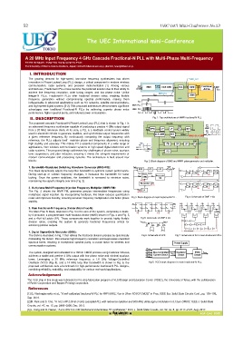
II. DESCRIPTION Fig. 1: Top architectures of MMFI fractional-N PLL.
The proposed cascade Fractional-N Phase-Locked Loop (PLL) that is shown in Fig. 1 is DIV-200
an advanced frequency synthesizer capable of producing a precise 4 GHz output signal VCO DIV-
200
from a 20 MHz reference clock. At its core, a PLL is a feedback control system widely f REF PFD CP LP DIV /200 RESET
DIV-
100
used in electronic circuits to generate, stabilize, and synchronize output frequencies with CLK GEN DIV RESET MMFI_PUL
a given reference frequency. By continuously comparing the output frequency with /100 BMS+CLK GEN
reference, the PLLs adjusts itself maintain phase and frequency alignment, ensuring VCO
high stability and accuracy. This makes PLLs essential components in a wide range of f REF Align FD CP LP MMFI_OUT
applications, from wireless communication systems to high-speed digital electronics and MMFI_PUL
radar systems. The proposed design addresses key challenges of phase noise, spurious MMFI_OUT MMFI_PUL PD
tone suppression, and jitter reduction, ensuring it meets the stringent requirements of
modern communication and processing systems. The architecture is built around four DLL
blocks: Fig. 2: Block diagram of BMS and MMFI pulse generator and multiplier.
1. Bandwidth-Modulated Switching Waveform Generator (BMS-WG): f MAIN PFD CP LPF VCO f OUT F OUT
This block dynamically adjusts the loop filter bandwidth to optimize system performance. D DFF1 Q D DFF2 Q D DFF3 Q M OUT D DFF4 Q
During start-up or sudden frequency changes, it increases the bandwidth for faster Dual Modulus Divider Prescaler QB QB M IN=1 QB M C=0 QB
locking. Once the system stabilizes, the bandwidth is narrowed to minimize noise, f DMD DMD f PR 1/N F IN
maintaining the signal's integrity over time (Fig. 2). d 0~d 3 F OUT
FA (4-bits) D FA D Q D Q D Q M OUT D Q
f 0~f 3 DFF1 DFF2 DFF3 DFF4
2. Multiphase Multi-Frequency Injection Frequency Multiplier (MMFI-FM): QB QB M IN=1 QB M C=1 QB
The Fig. 2 shows the MMFI-FM, generates precise intermediate frequencies using D FRAC F IN
s 0~s 3
multiphase signal injection. By incorporating feedback, this block reduces quantization
noise and improves linearity, ensuring accurate frequency multiplication and better phase Fig 3. Block diagram of main fractional-N PLL. Fig 4: Schematic of DMP 1-bit.
stability.
s 0 s 1 s 2 s 3
f PR f DMD A A A A
F IN F OUT F IN F OUT F IN F OUT F IN F OUT
B SUM B SUM B SUM B SUM
3. Main Fractional-N Frequency Divider (Main Frac-N): M OUT M IN M OUT M IN M OUT M IN M OUT M IN C IN C OUT C IN C OUT C IN C OUT C IN C OUT
The Main Frac-N block, depicted in Fig. 3 is the core of the system, comprising a divide- M C M C M C M C To FA (4-bits)
C OUT
d 0 d 1 d 2 d 3
by-4 prescaler, a programmable multi-modulus divider (MMD) shown in Figs. 4 and Fig. 5, Q DFF1 D Q DFF2 D Q DFF3 D Q DFF4 D
and a 4-bit full adder (FA). These components work together to provide highly flexible Fig 5: Schematic of DMP 4-bit.
F DMD
division ratios, enabling the system to generate fractional frequencies critical for V OUT_PFD V OUT_LP
achieving precise outputs. V B1 M 1 M 2 V B1 M 3 M 4
V SS V SS CLOCK DISTRIBUTION
4. Digital Sigma-Delta Modulator (DSM):
The DSM is illustrated in Fig. 7 that refines the fractional division process by dynamically Fig 6. Schematic of LPF. Fig 7. Schematic of in main fractional-N PLL.
modulating the divisor. This ensures high-frequency resolution and suppresses unwanted
spurious tones, resulting in exceptional spectral purity, a crucial factor for wireless and Power Supply
communication systems.
V BIAS
The system, designed and simulated in a 180nm CMOS process using Cadence Virtuoso, V OS1 Bias Controlled Oscillator PWM f VCO
V OS2 Current Circuit V VCT Circuit Circuit
achieves a stable and precise 4 GHz output with low phase noise and minimal spurious V OS3
tones. Leveraging a 20 MHz reference frequency, a 1.6 GHz Voltage-Controlled
Oscillator (VCO) (Fig. 8), and a 10 MHz loop filter bandwidth is shown in Fig. 6, the Fig 8. VCO block diagram in main fractional-N PLL.
proposed architecture sets a benchmark for high-performance fractional-N PLL designs,
combining reliability, scalability, and adaptability for various real-world applications.
Acknowledgement
The VLSI chip in this study was fabricated in the chip fabrication program of VLSI Design and Education Center (VDEC), the University of Tokyo, with the collaboration
of Rohm Corporation and Toppan Printing Corporation.
References
[1] G. Vlachogiannakis et al., “A self-calibrated fractional-N PLL for WiFi 6/802.11ax in 28nm FDSOI CMOS,” in Proc. IEEE Eur. Solid State Circuits Conf., pp. 105–108,
Sep. 2019.
[2] D. Park and S. Cho, “A 14.2 mW 2.55-to-3 GHz cascaded PLL with reference injection and 800 MHz delta-sigma modulator in 0.13µm CMOS,” IEEE J. Solid-State
Circuits, vol. 47, no. 12, pp. 2989–2998, Dec. 2012.
[3] L. Kong and B. Razavi, “A 2.4-GHz 6.4-mW fractional-N inductorless RF synthesizer,” IEEE J. Solid-State Circuits, vol. 52, no. 8, pp. 2117–2127, Aug. 2017.
ASP-DAC 2025