
Page 12 - 2024S
P. 12
UEC Int’l Mini-Conference No.52 5
for driving new-to-market wide-bandgap power
switching devices such as GaN power semicon-
ductor devices. The strong driving capability
due to the high source/sink current allows the
switch to turn off with a negative gate voltage
and low voltage oscillation, which is beneficial
in preventing false switch starts. [7].
The output signal of the fast current sensor is
processed by the operational amplifier and sent
to the reference terminal of the window com-
parator. Under normal circumstances, this ref-
erence voltage value is between the other two
preset input voltages of the window compara-
tor, and therefore the window comparator will
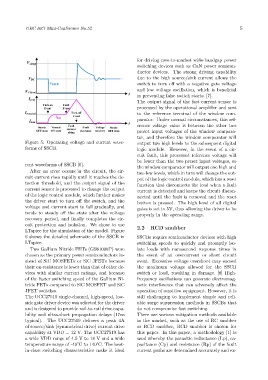
Figure 5: Operating voltage and current wave- output two high levels to the subsequent digital
forms of SSCB. logic module. However, in the event of a cir-
cuit fault, this processed reference voltage will
be lower than the two preset input voltages, so
rent waveforms of SSCB [6].
the window comparator will output one high and
After an error occurs in the circuit, the cir- two low levels, which in turn will change the out-
cuit current rises rapidly until it reaches the de- put of the logic control module, which has a reset
tection threshold, and the output signal of the function that disconnects the load when a fault
current sensor is processed to change the output current is detected and keeps the circuit discon-
of the logic control module, which further makes
nected until the fault is removed and the reset
the driver start to turn off the switch, and the
button is pressed. The high level of all digital
voltage and current start to fall gradually, and gates is set to 5V, thus allowing the driver to be
tends to steady off the state after the voltage properly in the operating range.
recovery period, and finally completes the cir-
cuit protection and isolation. We chose to use
LTspice for the simulation of the model. Figure 2.2 RCD snubber
6 shows the detailed schematic of the SSCB in SSCBs require semiconductor devices with high
LTspice. switching speeds to quickly and promptly iso-
Two Gallium Nitride FETs (GS61008P) were late loads with nanosecond response times in
chosen as the primary power semiconductors in- the event of an overcurrent or short circuit
stead of SiC MOSFETs or SiC JFETs because event. Excessive voltage overshoot may exceed
their on-resistance is lower than that of other de- the maximum voltage allowed for the SSCB
vices with similar current ratings, and because switch or load, resulting in damage. [8] High-
of the faster switching speed of the Gallium Ni- frequency oscillations can generate electromag-
tride FETs compared to SiC MOSFET and SiC netic interference that can adversely affect the
JFET switches. operation of sensitive equipment. However, it is
The UCC27519 single-channel, high-speed, low- still challenging to implement simple and reli-
side gate driver device was selected for the driver able surge suppression methods in SSCBs that
and is designed to provide rail-to-rail drive capa- do not compromise fast switching.
bility and ultra-short propagation delays (17ns There are various mitigation methods available
typical). The UCC27519 delivers a peak 4A in the market, such as the use of RC snubber
of source/sink (symmetrical drive) current drive or RCD snubber, RCD snubber is chosen for
capability at VDD = 12 V. The UCC27519 has this paper. In this paper, a methodology [1] is
a wide VDD range of 4.5 V to 18 V and a wide used whereby the parasitic inductance (Lp), ca-
temperature range of -40°C to 140°C. The best- pacitance (Cp) and resistance (Rp) of the fault
in-class switching characteristics make it ideal current paths are determined accurately and ex-