
Page 13 - 2024S
P. 13
6 UEC Int’l Mini-Conference No.52
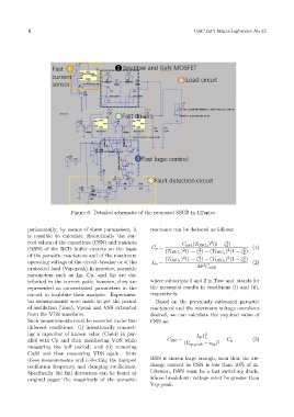
Figure 6: Detailed schematic of the proposed SSCB in LTspice.
perimentally; by means of these parameters, it reactance can be deduced as follows:
is possible to calculate theoretically the cor-
rect values of the capacitors (CSN) and resistors C add (T OSC 2 ) (1 − ζ )
2
2
2
(RSN) of the RCD buffer circuits on the basis C p = 2 2 2 2 (1)
1
2
(T OSC 1 ) (1 − ζ ) − (T OSC 2 ) (1 − ζ )
of the parasitic reactances and of the maximum 2 2 2 2
1
2
operating voltage of the circuit-breaker or of the L p = (T OSC 1 ) (1 − ζ ) − (T OSC 2 ) (1 − ζ ) (2)
2
protected load (Vsp-peak).In practice, parasitic 4π C add
parameters such as Lp, Cp, and Rp are dis-
tributed in the current path; however, they are where subscripts 1 and 2 in Tosc and stands for
represented as concentrated parameters in the the measured results in conditions (i) and (ii),
circuit to facilitate their analysis. Experimen- respectively.
tal measurements were made to get the period Based on the previously estimated parasitic
of oscillation (Tosc), Vpeak and VSS extracted reactances and the maximum voltage overshoot
from the VDS waveform. desired, we can calculate the required value of
Such measurements must be recorded under two CSN as:
different conditions: (i) intentionally connect-
ing a capacitor of known value (Cadd) in par- L p I 2
allel with Cp and then monitoring VDS while C SN = L − C p (3)
(V sp-peak − v in ) 2
measuring the toff period; and (ii) removing
Cadd and then measuring VDS again. from
these measurements and collecting the damped RSN is chosen large enough, such that the dis-
oscillation frequency and damping coefficients, charge current in CSN is less than 10% of iL.
Specifically the full derivation can be found at Likewise, DSN must be a fast switching diode,
original paper.The magnitude of the parasitic whose breakdown voltage must be greater than
Vsp-peak.