
Page 14 - 2024S
P. 14
UEC Int’l Mini-Conference No.52 7
Figure 7: Characterization of GaN de-
vices(GS61008P) used under independent test-
ing
3 Results
By scanning the DC characteristics of the device
in LTspice, the simulation circuit is shown in
the figure, and the following results are obtained
In the Figure 7, where the IDS on the vertical
axis and VGS on the horizontal axis, different
coloured lines represent the different VDS, and (a)
the slope represents the RDS.
It can be seen that the minimum RDS of the
GS61008P is 14m. Compared to the minimum
loss of the device mentioned earlier, it is reduced
by 60 %.
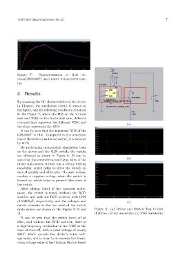
By performing independent simulation tests
on the driver and the GaN switch, the results
are obtained as shown in Figure 8. It can be
(b)
seen that the symmetrical and large value of the
driver sink/source current has a strong driving
capability, which helps to drive the switch on
and off quickly and efficiently. The gate voltage
reaches a negative voltage when the switch is
turned on, which helps to prevent false start of
the switch.
After adding 15mH of line parasitic induc-
tance, the circuit is tested without the RCD
snubber and with the RCD snubber with CSN
of 56000pF, respectively, and the voltages and (c)
circuit currents at the two ends of the switch
drain source are shown in the Figure 9 10 and Figure 8: (a) Driver and Switch Test Circuit
11. (b)Drive current waveforms (c) VGS waveforms
It can be seen that the switch turns off at
60ns, and without the RCD snubber, there is
a high-frequency oscillation in the VDS at the
time of turn-off, with a peak voltage of nearly
500V, which exceeds the device’s rated volt-
age value, and is close to or exceeds the break-
down voltage value of the Gallium Nitride-based